Transistors, Encapsulation, and the NOT Gate
So far you've flipped switches with the mouse — your finger standing in for the electricity. Real computers don't have tiny fingers. They use a switch that other electricity can flip: the transistor. In this lab you'll swap your switches for transistors, wrap your circuits up as reusable parts, and build a brand-new gate.
Overview
You'll replace the manual switches in MyAND and MyOR with transistors,
encapsulate each circuit with named inputs and an output, and build a new
one-input gate — the NOT gate.
Before you start
Open your MyAND and MyOR circuits from the last lab in Antares.
You've got it when…
- Both switches in
MyANDandMyORare replaced with transistors. - Each circuit has named inputs and an output that reads
0(notZ) when it should. -
MyNOTflips its input and matches the truth table.
Collaboration & AI
Work: On your own. A neighbor can help you find a menu; the wiring is yours.
AI — AIAS Level 1, No AI: Build and reason about the circuits yourself. What the levels mean.
Meet the Transistor
A transistor is an electronic version of the manual push switch. It has three pins. It forwards current from the Source (S) pin to the Drain (D) pin when voltage is applied to the Gate (G) pin.
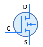
Your first task is to replace the manual switches in MyAND and MyOR with
transistors. For each switch:
- Remove the switch from your design.
- Replace it with a Transistor N-type (not P-type!) from the Net folder.
- Connect the S pin to the voltage-source side and the D pin to the LED side.
- Leave the G pin disconnected — we'll wire it in the next section.
Tip
Press Cmd+R to rotate the transistor — or any selected component — while you're in edit mode.
Encapsulation
Instead of flipping switches with the mouse, we'll drive the G pins with an electrical signal. We also want to reuse each circuit as its own component in a bigger design. Antares lets us define a circuit's inputs and outputs for exactly this.
For each transistor:
- Add a Circuit Input from the Input folder.
- Connect it to the transistor's G pin.
- Rename it: with the input selected, edit the Name property in the Properties sheet. Name your two inputs A and B.
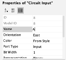
For the output:
- Remove the LED.
- Replace it with a Circuit Output from the Output folder.
Here is one possible solution for MyAND:
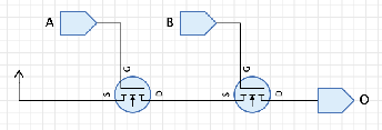
Try simulating it. Click the Circuit Inputs to flip them on and off and watch the output.
Why does the output read Z?
The output reads Z, not 0, because it's floating — disconnected from
any signal when the transistors are off. To make it read 0 (and we want it
to!), we need a way to connect it to ground (low) whenever it isn't
connected to voltage (high) through the transistors.
- Add a Pull Resistor from the Net folder just before the output.
Tip
Hold Option while hovering over the wire between the last transistor and the Circuit Output to create a short junction, then connect the Pull Resistor to the end of that junction.
Your MyAND circuit might look like this now. Simulate it again, confirm it
matches the AND truth table, then apply the same changes to MyOR.
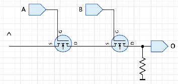
The Pull Resistor "pulls" the output down to ground when no voltage arrives from the transistors. When voltage is applied, the electricity takes the path of lower resistance straight to the output, bypassing the resistor.
The NOT Gate
Let's build one more circuit: an inverter, better known as a NOT gate. It
takes a single input and flips it — a 0 becomes a 1, and a 1 becomes a 0.
Complete a truth table for this gate based on that description.
MyNOT
| A | O |
|---|---|
Create a new circuit named MyNOT and build it with this recipe:
- Add a Pull Resistor from the Net folder.
- Select it and change the Pull Direction from LOW to HIGH in the Properties sheet (see Encapsulation if you need help finding it).
- Rotate the resistor so the arrow faces up (see Meet the Transistor for the rotation shortcut).
- Add a Transistor N-type from the Net folder.
- Connect the transistor's D pin to the end of the resistor.
- Add a Ground from the Net folder.
- Connect the Ground to the transistor's S pin.
- Add a Circuit Input from the Input folder.
- Rename the Circuit Input to A (see Encapsulation for renaming).
- Connect the Circuit Input to the transistor's G pin.
- Add a Circuit Output from the Output folder.
- Connect the Circuit Output to a wire junction between the transistor and the resistor (see Encapsulation for creating a junction).
Your solution should look like this.
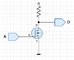
Simulate the circuit and confirm it works according to your truth table.
Turn It In
- Your completed
MyNOTtruth table (in your notebook). - A screenshot of each of your three circuits:
MyAND,MyOR, andMyNOT.
How It's Graded
This lab is worth up to 4 points. One score covers everything you turn in.
| Score | What it looks like |
|---|---|
| 4 — Excellent | All three circuits are transistor-driven with named inputs and a Circuit Output, every output reads 0 or 1 (never Z) in simulation, MyNOT matches its truth table, and the truth table is correct. |
| 3 — Above Average | All three circuits are built and behave correctly, with a minor gap — an unnamed input, one output still reading Z, or an untidy layout that still works. |
| 2 — Average | Two of the three circuits work, or all three are built but one misbehaves (wrong pull direction, transistor wired backward) and wasn't debugged. |
| 1 — Below Average | Only one circuit works, or the switches were never replaced with transistors. |
| 0 — Failing | Nothing turned in, or no evidence of transistor circuits. |